By George Milad
Uyemura International Corporation
Southington CT
PCBs of yesterday come nowhere close to matching the technologies and requirements of today’s PCBs and packages, and the continual move toward new technologies means the boards of tomorrow will bring even more exciting challenges. As the electronics industry continues its perpetual evolution toward faster, smaller, and cheaper, and with compliance issues always in the mix, process chemistry and equipment suppliers must constantly strive to meet these next-generation PCB and package designs.
Driving this evolution is the need for faster machines with greater emphasis on form factor and increasingly complex designs. RoHS compliance and WEEE environmental awareness also take their tolls on design complexity. Take for example the plethora of form factor capabilities and solutions of flex and rigid-flex boards — just one area of our industry — and you can begin to see the vast matrix of possibilities for all kinds of PCBs and packages.
With the challenges to meet these requirements come many opportunities for the next generation of plating and surface finish chemistries, or even new uses for the old reliables. Caught in the middle of this juggling act are chemical suppliers, who have at their disposal any combination of plating and via-fill chemistries to meet these requirements.
For instance, acid copper plating faces new challenges to plate higher aspect ratio boards with uneven trace designs, not to mention the challenges of filling vias for HDI. Surface finishes require better understanding and new products to meet the new high-temperature assembly conditions of lead-free electronics and to ensure the reliability of those solder joint.
What of metallization? It is imperative for metallization/desmear systems to cross over to the rigors of high-temperature processing for lead-free products, and must coexist with high-temperature laminates and lead-free solder alloys. What are the ideal metallization systems for polyimide flex and rigid-flex boards? Are the present systems adequate? Is there a need for something new?
This article provides a breakdown of available process chemistries, where they fit in the requirements of today’s most complex PCBs and packages. Because when you enter this brave new world, you must understand the available process chemistries and solutions and how they will meet your end customer’s needs.
Plating
To meet new market demands, PCB manufacturers are forced to seek new and advanced processes in every step of the manufacturing process. Metallization of the through hole and acid copper plating come under heavy scrutiny, as they constitute the processes that forms the traces and through hole connectivity, conveying the signal from end to end of the final device.
Palladium Metallization
A new metallization system based on palladium adsorption is being introduced, driven by the shortcomings of existing processes like electroless copper or carbon metallization. Palladium metallization is not new, but the new generation is different, as it addresses all the shortcomings of previous generations as well as alternate processes.
The new system is designed to meet the needs of flex and rigid-flex boards, where adhesive layers are always used in the lay-up. These layers are susceptible to attack by the high alkalinity used in electroless copper deposition.
This new generation provides a highly reduced process time minimizing exposure to alkalinity. It also has a unique conditioning system that makes the palladium adhere only to the polyimide dielectric and not to the copper. Carbon metallization processes require removal of carbon from the copper surface before plating, but this new system does not require etching the copper surface before electrolytic plating. Micro-etching the copper surface gave rise to wedge voids, reducing the reliability of the inner layer interconnect junctions in multilayer boards.
Acid Copper
The challenge for acid copper electroplating is to achieve good thickness distribution and surface uniformity without compromising the metallurgical properties (tensile strength and percent elongation) of the deposit. These properties become particularly important, as the plated copper is subjected to higher thermal stress during lead free solder assembly.
Manufacturers typically encounter problems with thickness distribution of acid copper in two primary areas: on the surface and in the plated through hole. On the surface, acid copper can cause over-plating of isolated traces (high current density areas) in comparison to the larger ground plane areas (low current density). In the hole, the challenge is to meet the minimum copper thickness requirements in the center of the high aspect ratio hole, otherwise known as throwing power.
Surface uniformity is sometimes plagued with the occurrence of nodules, which come from a variety of sources. Gold wire bonding applications have no tolerance to any level of nodulation.
New developments are helping to meet these challenges:
- New chemical additive packages for improved distribution
- Mass transfer improvements to compliment additives
- Nodule elimination by use of insoluble anode
- “Via Filling,” a specific application
High-Throw DC Plating
A new generation of “High Throwing Power” acid copper systems has come to the market in recent years. These baths are designed for today’s plating currents, which are lower than the traditional 25 - 30 ASF, which was common in the days of double-sided and simpler products.
High-throw baths are designed to give the desired physical properties at current densities as low as 5 ASF and as high as 20 ASF, with standard DC rectification. They produce bright ductile deposits.
These bath types are characterized by a specific combination of organic additive packages that include a unique leveling agent. The leveler plays a key role in improving throwing power, particularly when coupled with eductor (airless) agitation.
Figure 1:
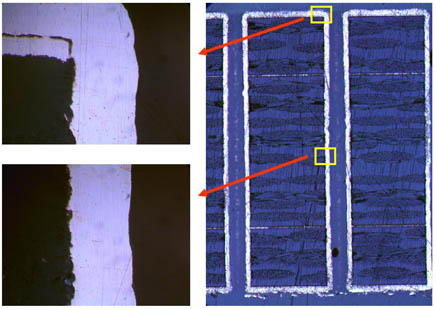
Figure 1 shows a 10:1 aspect ratio PTH plated at 10 ASF for 120 minutes, using a DC acid copper plating system.
Some of these baths can give a throwing power >80% for a 10:1 aspect ratio hole, plating at 15 ASF for 90 minutes, using DC rectification in a vertical dip tank application.
Via Fill Plating
To meet the demands of HDI, via fill plating is fast becoming a clear choice for connecting different layers in build-up technology (stacked vias and vias in pad). This provides overall improvement in long-term reliability of both PCBs and chip packages.
Pulse and DC plating via fill chemistries — many with new electrolytes — offer a series of advantages, as they do not require pulse rectification and avoid the complexity of managing a pulse wave. In addition, DC plating systems are stable and do not require constant regeneration of electrolytes used with pulse rectification.
Via filling is based on high-depositing ion concentration coupled with a low concentration of a leveling agent, in addition to carrier and the brightener additives. Most of these systems require optimized solution flow, enabling the leveler to accumulate on the surface, which inhibits plating while the bottom of the via continues to plate. Plating dynamics in the bottom of the hole are very different from those on the board surface, so as the hole fills, plating dynamics even out.
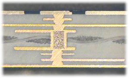
The new generation of via fill acid copper chemistries are designed to operate in DC mode, at 10 to 30 ASF, filling vias in under an hour using a standard plating cell with DC rectification. These systems are also capable of plating a hole during the via-fill plating process and have found applications in filling package channels and vias. Figure 2 shows sequential build up of stacked vias.
Figure 2:
Acid copper plating has come a long way since the early days of double- and single-sided PCBs, and it goes without saying that plating challenges will continue to increase as new product demands (lighter, smaller, more reliable) come to market. As one leading edge milestone is conquered, a new one is set.
The Finish is Only the Beginning
Surface finish evolution outpaces all chemical processes, because the complexity of design and environmental restrictions of lead- and halogen-free electronics force the industry to take a closer look at how existing finishes meet these requirements, as well as to continually generate new systems.
Surface finish is all about connectivity, whether it is in the form of a solder joint, wire bond, or even a contacting surface. Surface finishes fall into two categories depending on the kind of solder joint IMC formed, Ni/Sn IMC and Cu/Sn IMC. Electroless nickel immersion gold (ENIG) and electroless nickel electroless palladium immersion gold (ENEPIG) make a Ni/Sn IMC, while OSP, immersion silver, immersion tin, and direct immersion gold (DIG) all form Cu/Sn IMCs. Figure 3 shows the components of the IMC for both these categories.
Figure 3:
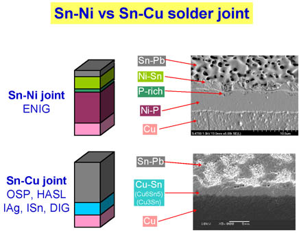
Ni/Sn IMC requires higher assembly temperature than Cu/Sn IMC and also has a phosphorous enriched layer at the interface. This is a natural component of any NI/Sn IMC formed on a nickel phosphorous deposit.
ENIG
ENIG is formed by the deposition of electroless nickel-phosphorous on a catalyzed copper surface, followed by a thin layer of immersion Gold. The IPC ENIG specification, IPC-4552, specifies 120 – 240 micro-inches (µins) of Ni with 2 – 4 micro-inches (µins ) of immersion gold.
ENIG is a very versatile surface finish. It is a solderable surface, aluminum wire bondable, and an excellent electrical contacting surface. It has excellent shelf life, in excess of 12 months, is easy to inspect (visual), and the thickness is easily verified by non-destructive XRF measurement. ENIG continues to gain market share, particularly after the understanding and virtual elimination of the “Black Pad” issue. The “Black Pad” occurs when a compromised nickel surface is corroded by prolonged exposure to the immersion gold deposition step.
A new gold chemistry developed in Japan designed to eliminate excessive corrosion of the nickel during gold deposition is now available. The mechanism of deposition is both immersion and autocatalytic — autocatalytic deposition is non corrosive.
ENEPIG
ENEPIG is formed by the deposition of electroless Ni (120 – 240 µins) followed by 4 – 8 µins of electroless Pd with an immersion gold flash (1 – 2 µins). ENEPIG is the finish with the widest latitude for a variety of applications. Sometimes referred to as the “Universal” finish, it was introduced in the mid ’90s, ENEPIG became known as the “Universal Finish” because of its usage versatility.
- soldering
- gold wire bondable
- aluminum wire bondable
- contacting
Although ENEPIG was introduced in the mid-‘90s, it did not take off as expected particularly in the area of soldering with the eutectic solder used at that time. The incompatibility of the lead with the palladium interfered with the formation of a uniform Ni/Sn IMC.
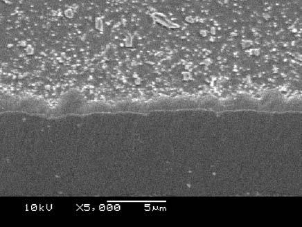
Fast forward to 2006 and ENEPIG has once again come under close scrutiny, as the industry evaluates its capabilities in lead-free assembly conditions. ENEPIG came through with flying colors as it formed one of the most robust solder joints with lead-free SAC type alloys. Extended solder joint life testing (see Figure 4) simulation using baking at 150°C for up to 1,000 hours was conducted, and shear ball testing showed no loss of solder joint strength. SEM studies and elemental analysis shows that the presence of the palladium in the joint interface dramatically reduces inter-metallic (IMC) propagation, making ENEPIG the leading choice finish for packages that require soldering and wire bonding with lead-free SAC type alloys.
Figure 4:
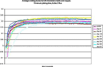
DIG
Direct immersion gold (DIG) on copper is a relatively new surface finish that shows a lot of promise in lead-free applications. This finish consists of plating 2 microinches (0.05 microns) of gold directly on the copper surface as a solderability preservative. The mechanism is a combination of immersion as well as electroless (autocatalytic) deposition, giving rise to a very tight lattice that greatly limits copper diffusion to the surface.
The graph (courtesy Photocircuits) in Figure 5 shows wetting balance curves for up to 877 days after deposition. The samples were stored in ambient lab conditions.
Figure 5:
One of the key applications for this finish is for PCBs designed for RF signal propagation. Due to the “skin effect,” the signal integrity may be compromised if a thick nickel layer is plated below the gold surface, as in the case of ENIG.
DIG forms a Cu/Sn IMC joint with both eutectic and SAC alloy lead-free solders. DIG shows a lot of promise, as it addresses the shortcomings inherent with other surface finishes. It will withstand multiple thermal excursions, the solder joint formed is free of interfacial voiding, it does not form any IMCs during storage before assembly, and it does not whisker.
DIG will also accept an electroless soft gold overcoat, and with as little as 15 micro inches (0.6 microns) the surface is ideal for gold wire bonding. DIG is primarily used in Japan and mostly in packaging applications, but it is gaining acceptance in the marketplace as designers and manufacturers become more familiar with its capabilities.
Immersion Silver
Although this finish is well established in the industry, the learning curve regarding handling, packaging, and storage was the biggest challenge in introducing immersion silver into the market. Additional research is ongoing to establish its viability with lead-free solders and soldering. As this surface finish establishes itself in the marketplace, its advantages and weaknesses become better understood. Of late some instances of excessive interfacial voiding were reported, but the phenomenon was well researched and its root causes were established. Minor process modifications were introduced to ensure that the manufacturer can stay clear of any conditions that could create the defect.
Immersion Tin
Immersion tin is also a well-established surface finish that has evolved through many generations of improvements. Due to its lubricity and thickness uniformity, immersion tin is an ideal choice for compliant pin and press-fit connector applications. As attractive as immersion tin may sound as a lead-free surface finish, the higher temperature requirements inherent with lead-free assembly have brought new challenges requiring changes in the specifications of immersion tin thickness.
Immersion tin has not caught up extensively in the industry, the two dominant limitations of immersion tin are IMC formation between the tin and underlying copper and the propensity of whisker growth when the tin is plated on copper. Research continues on both these fronts to define its best operating conditions. Additives have also been uncovered that would virtually eliminate whisker formation.
In the fast-evolving technological world in which we live, meeting today’s industry challenges and tomorrow’s requirements opens doors to opportunities where innovative companies have a chance to contribute and grow by investments in research and development to provide solutions to the ever-changing market demands for smaller, cheaper, lighter, and faster packages.
The regulations associated with RoHS and WEEE require new technologies that lead the industry into unexplored areas requiring new products to meet the unexpected challenges related to higher temperature requirements.
These are exciting times in our industry with plenty of demanding challenges and opportunities. As one leading-edge milestone is conquered, a new one is set.