Electroless Metal Deposition Processes Have Been Developed for LTCC Metallization that Yield Excellent Wire Bond Strengths and Solder Joint Reliability
By Don Gudeczaukas
Uyemura International Corporation
Ceramic substrates have been used for many years in the production of electronic circuits. Ceramic substrates generally exhibit superior thermal performance when compared to organic substrates for uses in electronic packages, although many organic packages are also used due to cost and circuit design considerations.
Ceramic materials used in electronic manufacturing include aluminum oxide, silicon nitride and aluminum nitride. Low-temperature co-fired ceramic (LTCC) substrates have become especially popular in the last 10 years. LTCC substrates are a mixture of alumina and glass, and are typically manufactured into multilayer substrates co-fired with low-resistance metals like copper or silver at firing temperatures of less than 1000ºC.
Glass material that is included with the ceramic lowers both the fusing point of the matrix and also the dielectric constant, thus enhancing performance (especially at higher frequencies).1 A cross-sectional view of a LTCC circuit is shown in Figure 1. LTCC manufacturing methods allow for the formation of blind vias, buried components and thru-hole vias.
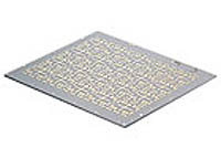
LTCC substrates are becoming more popular for a variety
of applications. Photo courtesy of TDK Corp., Phoenix, Ariz.
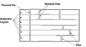
Figure 1. LTCC manufacturing methods allow for the formation of blind vias, buried components and thru-hole vias.
Finishing Requirements
Final finishes may be applied to the circuit pads for preservation of solderability or to serve as wire bonding pads. In many instances, the final finish is used for both purposes. In this case, care must be taken to ensure that the final finish can form a reliable solder joint while also allowing acceptable wire bonds. Optimization of the final gold plating thickness is crucial for optimum performance in the case of nickel-gold deposition.
In the process of forming the substrate circuitization, it is common that electrically isolated traces are created, thereby eliminating the possibility of electrolytic plating of final finishes unless some sort of bussing is incorporated that is subsequently partially removed after plating.
Electroless Deposition
Electroless deposition differs from electrolytic deposition in that no external supply of electrons (such as from a rectifier) are required. Electrolytic deposition requires the use of an externally connected DC rectifier, which supplies electrons for metal reduction at the cathodic surface. Electroless deposition utilizes a chemical reducing agent that supplies electrons for metal deposition at a catalytic surface. Examples of chemical reducing agents are formaldehyde for electroless copper deposition and sodium hypophosphite for electroless nickel deposition.
Two common electroless final finishes for ceramic packages are nickel-gold or nickel-palladium-gold. In certain high-frequency applications, the nickel layer may be avoided. The initial metal layer on the ceramic substrate and the glass materials blended with the aluminum oxide determine the required pretreatment prior to electroless nickel and gold (ENIG) or electroless nickel- electroless palladium-gold (ENEPIG) deposition for LTCC substrates. Materials in the glass portion of the LTCC substrate can sometimes affect the metal plating process and must be cleaned from the surface prior to plating.
Materials such as zinc, bismuth and lead, which are used to lower the fusing temperature, may affect the plating processes either by causing background plating (plating onto the ceramic substrate) or non-uniform nickel deposition onto silver metallization. In some cases, these metals are partially removed from the surface layer prior to plating. The cleaning process typically involves the use of a glass etch and cyanide dipping.
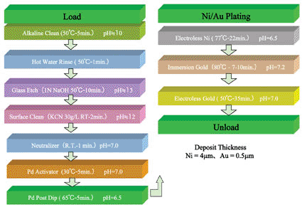
Figure 2. LTCC plating process for a Ni-Au plate (Ag metallized).
As mentioned previously, electroless nickel is not catalytic to the starting metal layer and, as a result, a catalyst is normally deposited onto the starting metal layer to facilitate electroless nickel deposition. Once the electroless nickel solution begins to deposit, the nickel metal builds upon itself at a controlled rate. An example of pretreatment for a silver metallized LTCC substrate is shown in Figure 2. The ceramic substrate and metallization layer determines the course of pretreatment.
In the case of silver metallization, a common conductor used with LTCC substrates, a neutral pH palladium catalyst solution is used since it is critical to ensure that no etching or lifting of the silver metallization occurs. Copper metallized substrates usually require an acidic palladium catalyst prior to electroless nickel deposition.
Once the metallization has been properly catalyzed, the substrates are immersed into the electroless nickel plating solution. Electroless nickel solutions typically operate at solution temperatures in the range of 77-90ºC and operate at mildly acidic solution pHs. Nickel deposit thicknesses typically range from 100-300 microinches, depending on the circuit requirements. During the nickel deposition, a portion of the reducing agent co-deposits with the nickel to form a crystalline or semi-amorphous compound, depending on the reducing agent of choice. The reducing agent typically is deposited in the 3-10% by weight range, with phosphorus being a typically co-deposited material.
Precious Metal Finishes
Precious metals are deposited onto the nickel surface to prevent the nickel from oxidizing (thus preserving a solderable surface) and optionally to serve as a gold wire bonding surface. Either gold or palladium plus gold are used as the final finish top coating. The nickel-gold or nickel-palladium-gold layers exhibit excellent heat resistance for multiple thermal cycles at assembly, especially for lead-free solders. For finishes using gold only as the final layer (ENIG), an immersion gold layer is deposited onto the electroless nickel.
An immersion deposit is simply a galvanic displacement reaction whereby nickel is dissolved from the surface of the deposit and gold replaces nickel at the surface. The nickel dissolution provides the electrons needed for gold deposition at the surface. Two atoms of gold are normally deposited for each atom of nickel dissolved at the surface according to the reaction:
2Au+ + Ni0 › 2Au0 + Ni++
This immersion gold reaction is normally self-limiting to approximately 0.1µm total thickness. As the available sites on the nickel surface are coated with gold, the immersion reaction slows; typically, the rate of deposition decreases to a very low rate after approximately 15 minutes. Following immersion gold plating, an optional electroless gold process may be used to increase gold thickness for wire bonding applications.
Two basic electroless gold processes are prevalent in the industry today. The first type of electroless process deposits gold from an alkaline solution using gold cyanide as the gold complex and either dimethyl amine borane or sodium borohydride as the reducing agents. The second type of electroless process deposits gold from a neutral pH solution using a gold-sulfite complex and an organic reducing agent. Both types of electroless gold can provide a thick, uniform, non-porous gold layer for wire bonding applications.
Another option for precious metal finishes involves the use of electroless palladium and a flash of gold over the electroless nickel deposit (ENEPIG). Thicknesses of the palladium are generally in the 0.05-0.1 µm range, followed by a thin coating of gold in the 0.025-0.4 µm range. The palladium serves to minimize possible nickel diffusion and also minimize intermetallic growth in Pb-free assembly. ENEPIG finishes are gaining interest due to the decreased thickness of gold required compared to traditional electroless nickel-electroless gold (ENAG) finishes.
Test Results
Several studies have been performed comparing the functional performance of ENEPIG and ENIG/ENAG deposits, especially with Pb-free solders. Figure 3 shows the comparative gold wire bonding pull strengths for ENAG ENEPIG deposits after heat-conditioning the samples at 175ºC for 16 hours. It can be seen that excellent wire bond pull strengths were found regardless of gold or palladium thickness. Thinner gold deposits with ENAG finishes did exhibit slightly lower wire bond pull strengths due to some diffusion of nickel to the surface during heat aging.
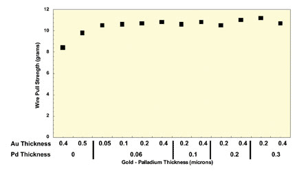
Figure 3. Wire bond test results after baking at 175ºC for 16 hours (average readings).
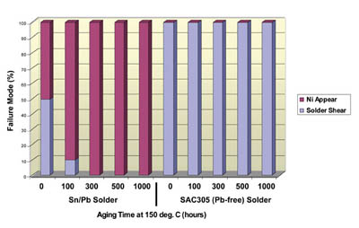
Figure 4. Solder ball pull test results for ENEPIG Sn/Pb solder vs. Pb-free solder.
In addition, solder joint reliability tests were performed on ENEPIG deposits and compared to ENIG deposits using Pb-free SAC305 solder and eutectic Sn/Pb solder. Results indicated that ENEPIG deposits coupled with eutectic Sn/Pb solder resulted in poorer solder joint reliability after thermal aging compared to ENIG deposits. ENEPIG coupled with SAC305 solder yielded excellent solder joint reliability throughout the range of thermal aging, and actually surpassed the reliability of ENIG deposits (see Figure 4).
LTCC substrates are becoming more popular for a variety of applications. Electroless metal deposition processes have been developed for LTCC metallization that yield excellent wire bond strengths and solder joint reliability.