By George Milad
Uyemura International Corporation
Southington CT
The elimination of lead from electronic devices as mandated by RoHS (Restriction of Hazardous Substance) is changing the playing field for everyone involved in the printed circuit industry.
On the PCB level, OEMs have the brunt of dealing with the change; designers are always pushing the limits of the industry’s capabilities to meet the requirements of their newer designs. Presently, the push back is on what the industry is capable of delivering under the new directive.
Contract manufacturers are busy adapting their equipment and procedures. The new solder is more corrosive to copper and to equipment, they had to set new inspection criteria, ensure no cross-contamination with leaded components and establish new documentation and material declarations.
Manufacturers are dealing with new materials that can withstand the higher temperature of assembly of lead-free SAC alloys. There is a learning curve and all are scrambling to stay with it, let alone ahead of it.
Suppliers at the bottom of the chain, whether they supply laminate, solder, equipment, or plating chemistry, have been preparing and aligning their product offerings to meet the compliance deadline and beyond.
Chemical supplier R & D departments have been very busy defining the effect of the new regulations on their products, specifically in the area of surface finishing.
Surface finish products have been on the fast track of evolution just to meet the complexity of newer designs (lighter, faster, smaller) as handheld devices like i-pods, smart-phones, PDA’s, digital cameras, camcorders, scanners etc. continue down the form factor path. The new challenge is RoHS compliance and the need to have lead-free finishes and more important lead-free compatible finishes.
Surface finish is about connectivity. It is the surface which either protects or forms the connection from the board to a device. Today there is an impressive line-up of surface finish products in use as eutectic Sn/Pb HASL replacements. The list includes: electroless nickel/ immersion gold, electroless gold, electroless palladium, immersion silver, immersion tin, OSP, as well as DIG direct gold on copper.
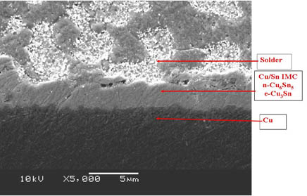
The surface finishes available fall into two categories based on the type of intermetallic formed in the solder joint, namely Cu/Sn intermetallic (IMC), and Ni/Sn (IMC). The Ni/Sn IMC requires a higher temperature and extended dwell at temperature during assembly.
Cu/Sn Intermetallic Solder Joints
Organic Solderability Preservatives (OSP)
OSPs form a CuSn IMC which is robust and well understood. It comes in thin and thick versions, is relatively inexpensive, and is easily applied. On the flip side, OSPs are limited in the number of heat cycles that can be endured at assembly; some OSPs require a nitrogen atmosphere at assembly, and they are also not suitable for wire bonding or as a contacting surface. However, with the new lead-free high temperature, a new generation of OSP products is being developed. These products must withstand the higher temperature thermal excursions and still protect the copper, to allow the solder to wick and fill the holes in the final wave soldering assembly step. Suppliers are developing new generations of OS’s to meet the challenges of Pb-free.
Immersion Tin
Immersion tin is also a well-established surface finish that has evolved through many generations of improvements. Due to its lubricity and thickness uniformity, immersion tin is an ideal choice for compliant pin and press-fit connector applications. As attractive as immersion tin may sound as a lead-free surface finish, the higher temperature requirements inherent with lead-free assembly have brought new challenges requiring changes in the specifications of immersion tin thickness. The IPC immersion tin specification, IPC-4554, specifies a minimum of 40 micro inches to ensure a minimum of six months shelf life without Cu/Sn IMC at the soldering surface. Lower thicknesses are accepted if approved by both user and supplier.
Immersion tin has not caught on extensively in the North American industry; the two dominant limitations of immersion tin are IMC formation between the tin and underlying copper and the propensity of whisker growth when the tin is plated on copper. Research continues on both these fronts to define its best operating conditions. Additives have also been uncovered that would virtually eliminate whisker formation.
Immersion Silver
Although this finish is well established in the industry, the learning curve regarding handling, packaging, and storage was the biggest challenge in introducing immersion silver into the market. The IPC immersion silver specification, IPC-4553, specifies a minimum of 5 micro inches typically 8 – 12 micro inches as measured on a 60 X 60 mil pad. Additional research is ongoing to establish its viability with lead-free solders and soldering. As this surface finish establishes itself in the marketplace, its advantages and weaknesses become better understood. Recently, some instances of excessive interfacial voiding were reported, but the phenomenon was well researched and its root causes were established. Minor process modifications were introduced to ensure that the manufacturer can stay clear of any conditions that could create the defect.
Direct Immersion Gold (DIG)
Direct immersion gold (DIG) on copper is a relatively new surface finish that shows a lot of promise in lead-free applications. This finish consists of plating 2 micro-inches (0.05 microns) of gold directly on the copper surface as a solderability preservative. The mechanism is a combination of immersion as well as electroless (autocatalytic) deposition, giving rise to a very tight lattice that greatly limits copper diffusion to the surface.
One of the key applications for this finish is for PCBs designed for RF signal propagation. Due to the “skin effect,” the signal integrity may be compromised if a thick nickel layer is plated below the gold surface, as in the case of ENIG.
DIG forms a Cu/Sn IMC joint with both eutectic and SAC alloy lead-free solders. DIG shows a lot of promise, as it addresses the shortcomings inherent with other surface finishes. It will withstand multiple thermal excursions, the solder joint formed is free of interfacial voiding, it does not form any IMCs during storage before assembly, and it does not whisker.
DIG will also accept an electroless soft gold overcoat, and with as little as 15 micro inches (0.6 microns) the surface is acceptable for gold wire bonding. DIG is primarily used in Japan and mostly in packaging applications, but it is gaining acceptance in the marketplace as designers and manufacturers become more familiar with its capabilities.
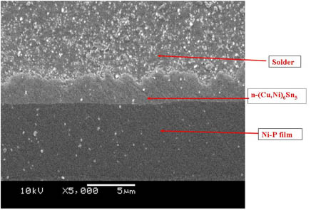
Ni/Sn Intermetallic Solder Joints
Electroless Nickel Immersion Gold (ENIG)
ENIG is formed by the deposition of electroless nickel-phosphorous on a catalyzed copper surface, followed by a thin layer of immersion Gold. The IPC ENIG specification, IPC-4552, specifies 120 – 240 micro-inches (µins) of Ni with 2 – 4 micro-inches (µins) of immersion gold.
ENIG is a very versatile surface finish. It is a solderable surface, aluminum wire bondable, and an excellent electrical contacting surface. It has excellent shelf life, in excess of 12 months, is easy to inspect (visual), and the thickness is easily verified by non-destructive XRF measurement. ENIG continues to gain market share, particularly after the understanding and virtual elimination of the “Black Pad” issue. The “Black Pad” occurs when a compromised nickel surface is corroded by prolonged exposure to the immersion gold deposition step.
A new gold chemistry developed in Japan designed to eliminate excessive corrosion of the nickel during gold deposition is now available. The mechanism of deposition is both immersion and autocatalytic (autocatalytic deposition is non corrosive).
Electroless Nickel, Electroless Palladium,
Immersion Gold (ENEPIG)
ENEPIG is formed by the deposition of electroless Ni (120 – 240 micro inches) followed by 4 – 8 micro inches of electroless Pd with an immersion gold flash (1 – 2 micro inches). ENEPIG is the finish with the widest latitude for a variety of applications. ENEPIG is sometimes referred to as the “Universal” finish, because of its usage versatility. ENEPIG is suitable for soldering, gold wire bonding, aluminum wire bonding, and contact resistance.
ENEPIG was originally introduced in the mid-‘90s, it did not capture a significant share of the market as expected. Recent ball shear data indicates an incompatibility with eutectic solder; the incompatibility of the lead with the palladium interferes with the formation of a uniform Ni/Sn inter-metallic (IMC).
The RoHS requirements of lead-free has made it necessary once again to revisit all available surface finish options and ENEPIG has again come under close scrutiny, as the industry evaluated its capabilities using lead-free assembly conditions. ENEPIG came through with flying colors as it formed one of the most robust solder joints with lead-free SAC type alloys. Extended solder joint life testing simulation using baking at 150oC for up to 1,000 hours was conducted, and shear ball testing showed no loss of solder joint strength. SEM studies and elemental analysis shows that the presence of the palladium in the joint interface dramatically reduces inter-metallic (IMC) propagation, making ENEPIG the leading choice finish for packages that require soldering and wire bonding with lead-free SAC type alloys.
As we meet the evolutionary challenges associated with new technologies, smaller pads, higher frequency signals, tighter controlled impedance, wire bonding etc. The eliminating of lead associated with the RoHS requirements becomes just one more evolutionary cycle driven by environmental regulation, not by leading edge technology. Surface finishes have always been an active process in PWB manufacturing affected by the changing world of electronics.
Evolutionary change will continue to face all technologies, creating new challenges and opportunities for nimble companies that are eager to adapt to ever-changing requirements by making wise choices. Two facts remain unchanged; there is not one surface finish that fits all applications, and not all chemistries are created equal. So, we must always remember, technology sophistication demands wise choices in utilizing the proper surface finish designed for the specific product's end use.