By Patrick Valentine, PhD
Uyemura International Corporation
Southington CT
Abstract
Soldering transforms bare printed circuit boards (PCBs) into functional electronic assemblies. Poor-quality soldering is costly. This paper explores the holy trinity of soldering: Clean, Solder, and Heat. In this context, identifying surface contaminants, applying solder paste, and using a proper reflow profile are discussed. Strict control of the holy trinity reduces frustrations, rework, and potential field failures, enabling world-class quality, “on target with minimal variation.”
Keywords: holy trinity, solderability, nonwetting, dewetting, surface analysis, SMT, ENIG
Introduction
Solderability is a metal’s ability to be wetted by molten solder. Two parameters define solderability: wetting time (the rate at which solder penetrates the coating, e.g., immersion gold, and begins bonding to the basis metal, e.g., electroless nickel) and wetting force (the quality of contact, liquid spreading, between the solder and the basis metal). Long wetting times suggest dirty surfaces, while low wetting force indicates basis metal oxidation. Solderability encompasses both the speed and quality of wetting [1].
The soldering process has two common defects: nonwetting and dewetting. Nonwetting is when molten solder partially adheres, leaving the basis metal exposed (see Figure 1). Dewetting occurs when solder initially coats a surface, then recedes, leaving mounds separated by thin films with the basis metal not exposed (see Figure 2). As stipulated in J-STD-001J, unassembled printed circuit boards must meet IPC J-STD-003D. Nonwetting and/or dewetting in excess of 5% of the soldered pad area is non-conforming [2, 3]. Therefore, it’s crucial PCBs are clean pre-assembly.
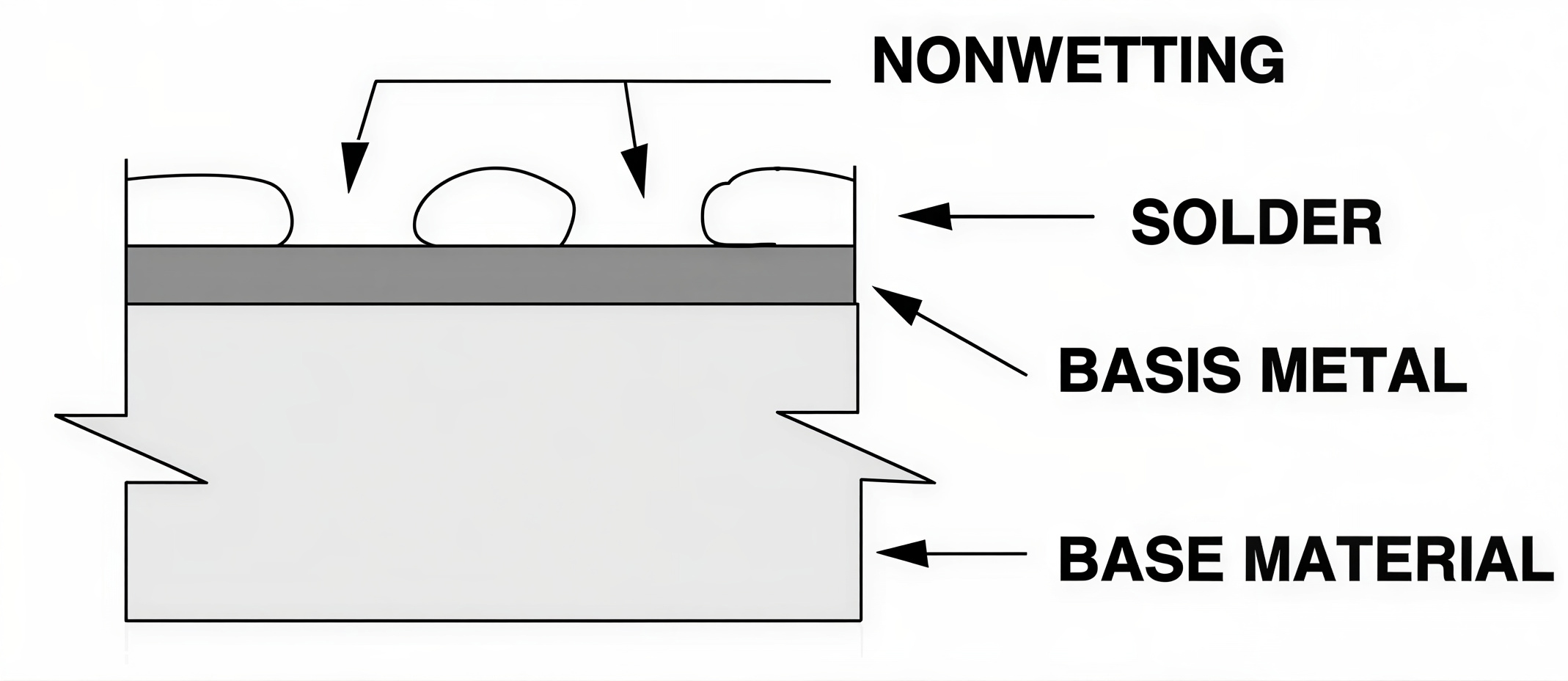
Figure 1. Non-wetting.
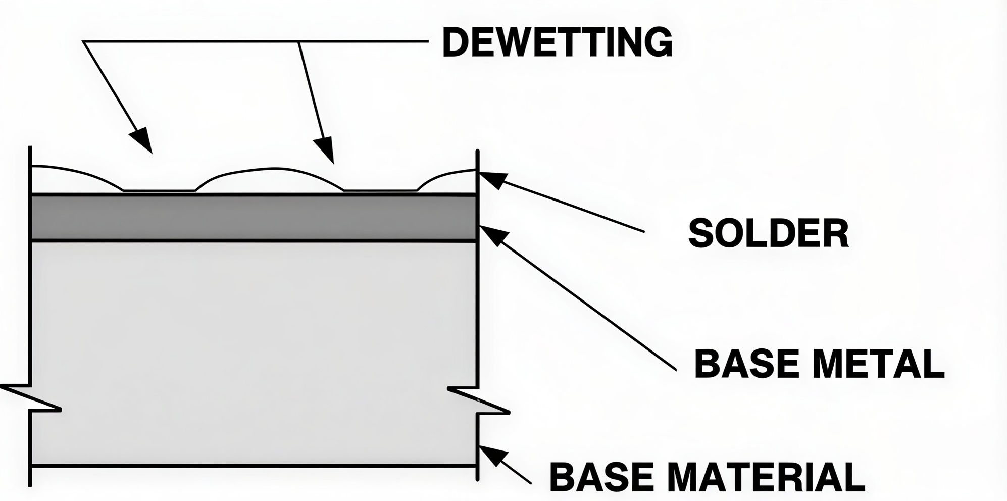
Figure 2. De-wetting.
IPC-A-610J lists several post-assembly soldering anomalies. These anomalies include exposed basis metal, pin holes/blow holes/voids, incomplete solder paste reflow, nonwetting, cold connection, dewetting, excess solder (balls, bridging, webbing/splashing), disturbed solder, cooling lines and secondary reflow, fractured solder, solder projections, fillet lift, and hot tear/shrink hole [4].
With these defects in mind, it is essential to recognize that successful solder connections require attention to three critical elements. The next section introduces the holy trinity: Clean, Solder, and Heat.
Clean
The first member of the trinity is Clean. Contaminants such as organics, oxides, oils, and soldermask residues can impede good wetting and the formation of an intermetallic compound (IMC) bond between the basis metal surface and the molten solder. Compounding the cleanliness problem are poor handling or storage conditions. Solderability can be affected by even low levels of surface and subsurface contaminants. Identifying surface contaminants can be challenging.
The EAG SMART (Spectroscopy and Microscopy Analytical Resolution Tool) Chart offers a concise visual reference for comparing analytical techniques. One can compare the detection limits and analytical resolutions of dozens of techniques used for materials characterization, surface evaluation, and purity surveys, as shown in Figure 3 [5].
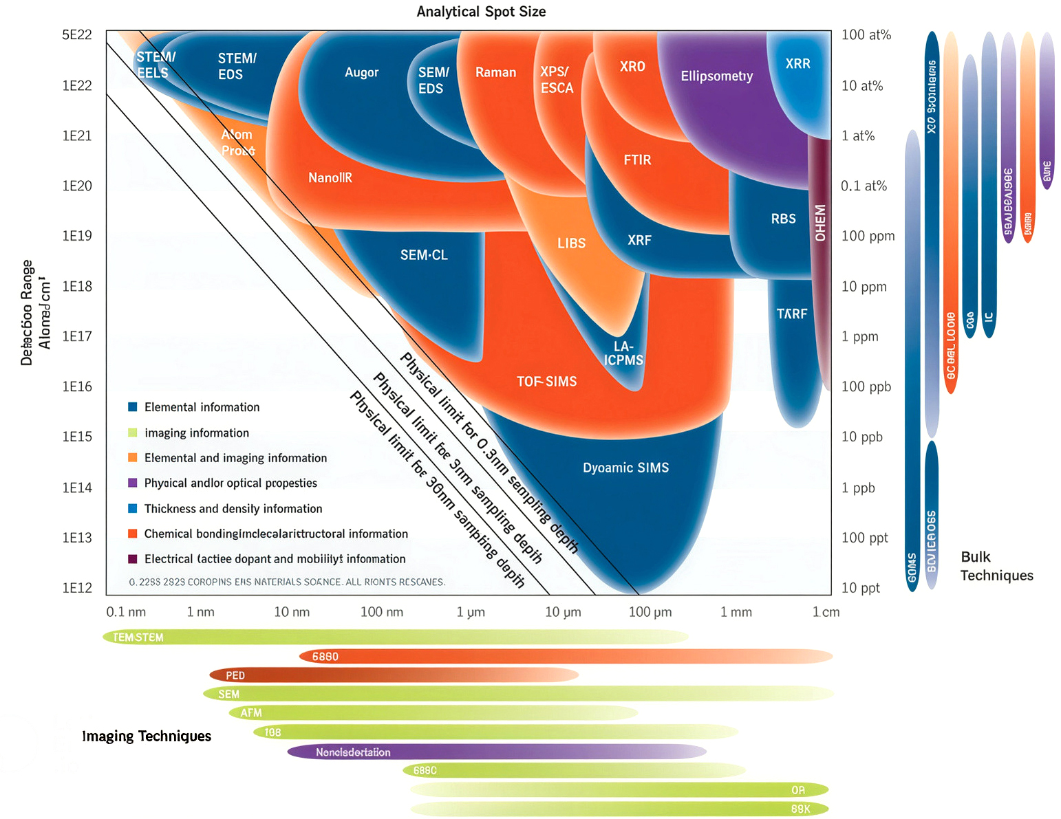
Figure 3. SMART (Spectroscopy and Microscopy Analytical Resolution Tool) Chart.
The SMART chart in Figure 3 depicts analytical resolution vs. detection limits. The x-axis lists the resolution, while the y-axis lists the detection limit. As you move from right to left on the x-axis, the resolution becomes finer. Simply stated, this is the lateral resolution, or the distance over which changes in composition can be separately established with confidence (spot size). As you move from top to bottom on the y-axis, detection limits become finer. Simply stated, the detection limit is the lowest concentration a technique can reliably detect. The left-hand side of the y-axis is in atoms/cm3, while the right-hand side is in various units. The atoms/cm3 is related to PPM via Equation 1 [5, 6].
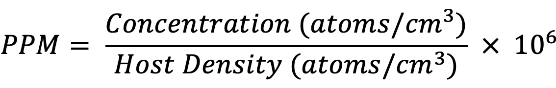
Equation 1. PPM relationship to atoms/cm3.
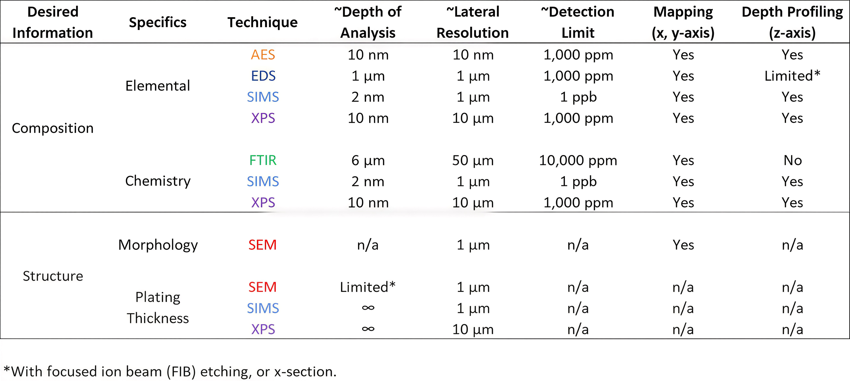
Common surface analysis techniques include AES, FTIR, EDS, SEM, SIMS, and XPS (see Table 1). Each method has advantages and disadvantages, which are compared as a quick reference in Table 2 based on the desired information [5, 6]. Following this, an example utilizing ToF-SIMS is provided.
Table 1. Common surface analysis techniques.
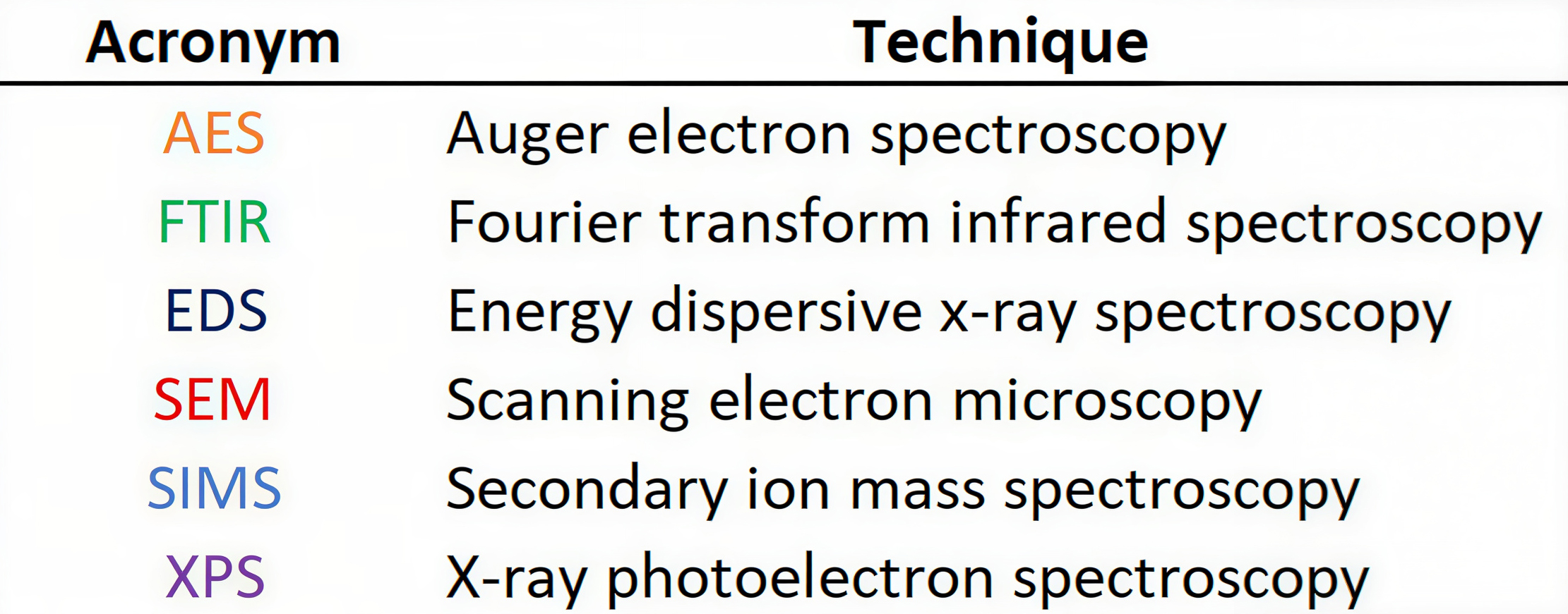
Table 2. Quick reference comparison of common surface analysis techniques.
Time-of-Flight Secondary Ion Mass Spectrometry (ToF-SIMS) analyzes surfaces by focusing a pulsed ion beam to generate secondary ions. This reveals the molecular, inorganic, and elemental species present at the top surface 1-2 nanometers (nm). This spectrometry method minimizes surface damage, making it ideal for detecting surface contaminants. Depth profiling is also possible. Figure 4 shows a stained ENIG surface; Figures 5 and 6 show ToF-SIMS analyses.
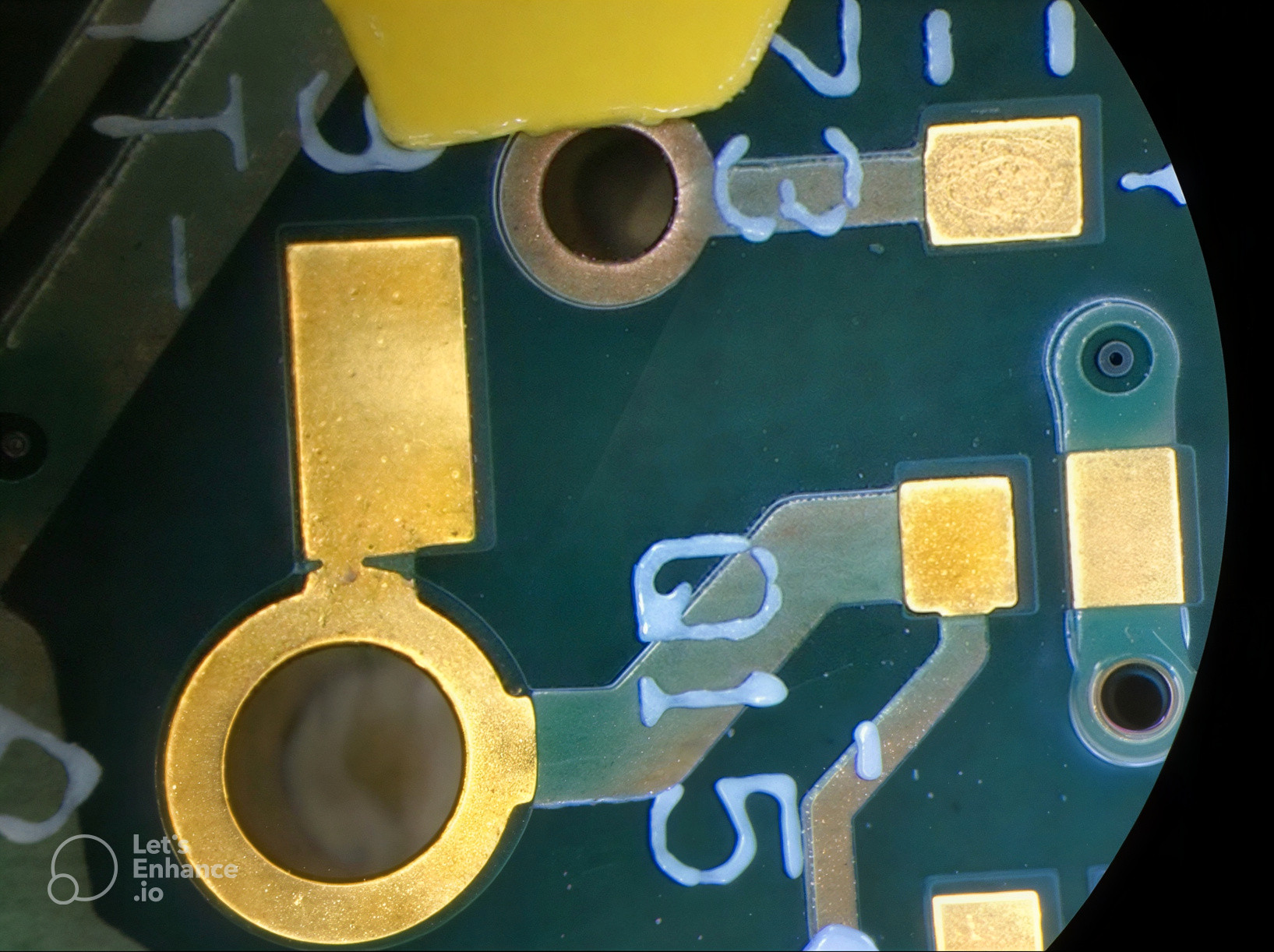
Figure 4. Stained electroless nickel immersion gold (ENIG) surface
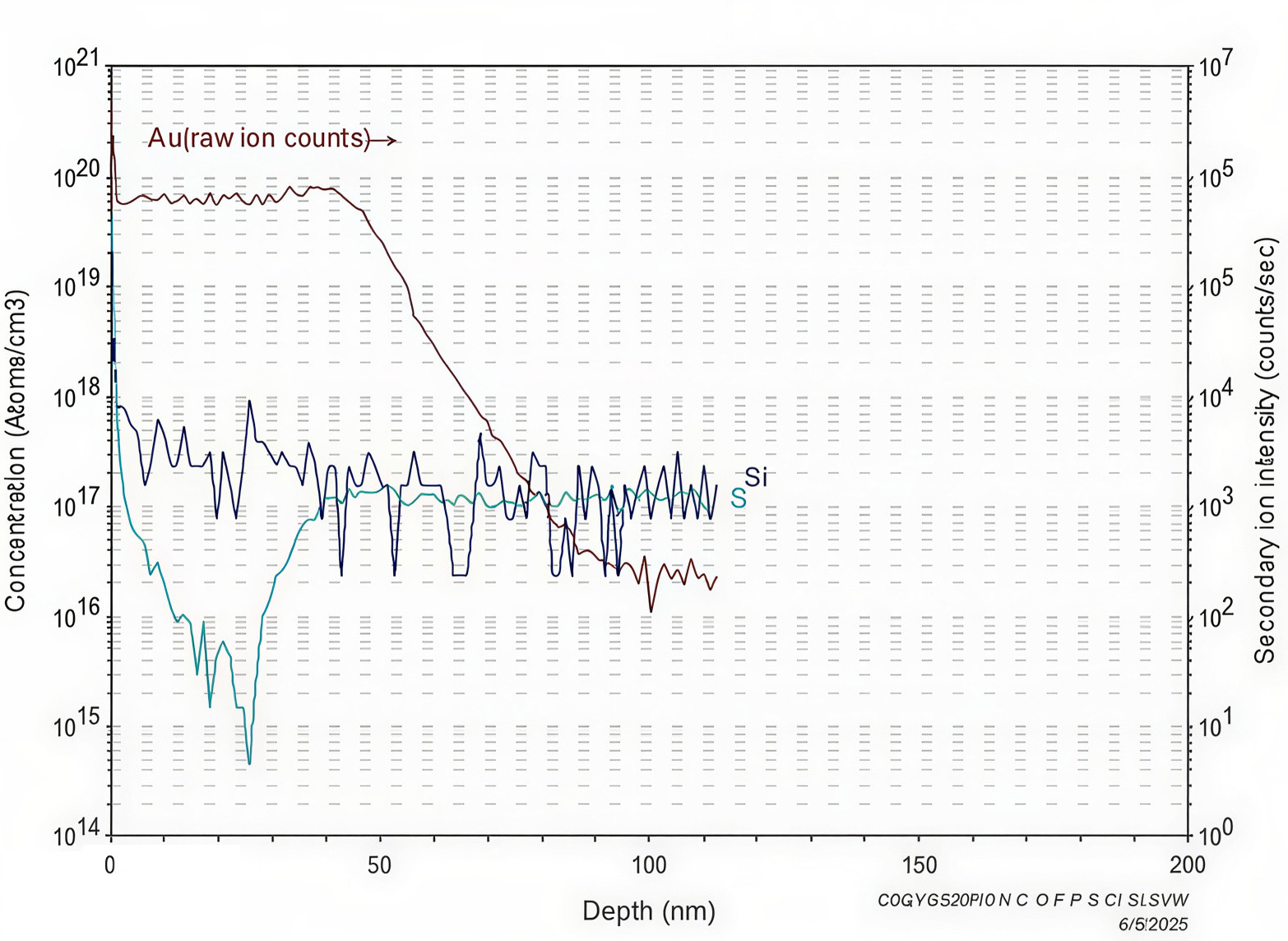
Figure 5a. TOF-SIMS elemental species surface analysis.
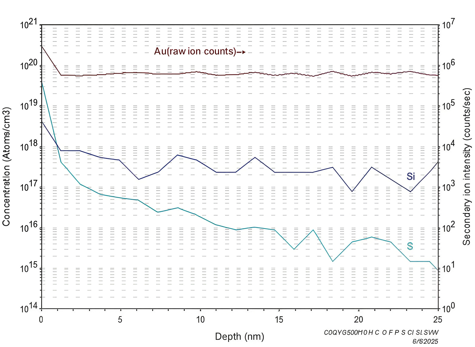
Figure 5b. TOF-SIMS elemental species surface analysis.
Commentary on Figures 5a and 5b: In addition to gold, several elemental species are present. Of particular concern are sulfur (S) and silicon (Si), which were found in higher concentrations at the gold surface’s uppermost nanometers, as shown by the elevated atom density/cm3 on the graph’s left side. Both elements can hinder solder wetting. The silicon, detected in positive ion mode (spectra is not shown), is attributed to polydimethylsiloxane (PDMS). Polydimethylsiloxane compounds are used in various products, such as lubricants, adhesives, release agents, pump oil, and skincare products. The presence of sulfur, silicon, and PDMS on the gold surface indicates possible issues with rinsing, handling, packaging, or storage. These contaminants can negatively impact soldering, and should be considered process indicators.
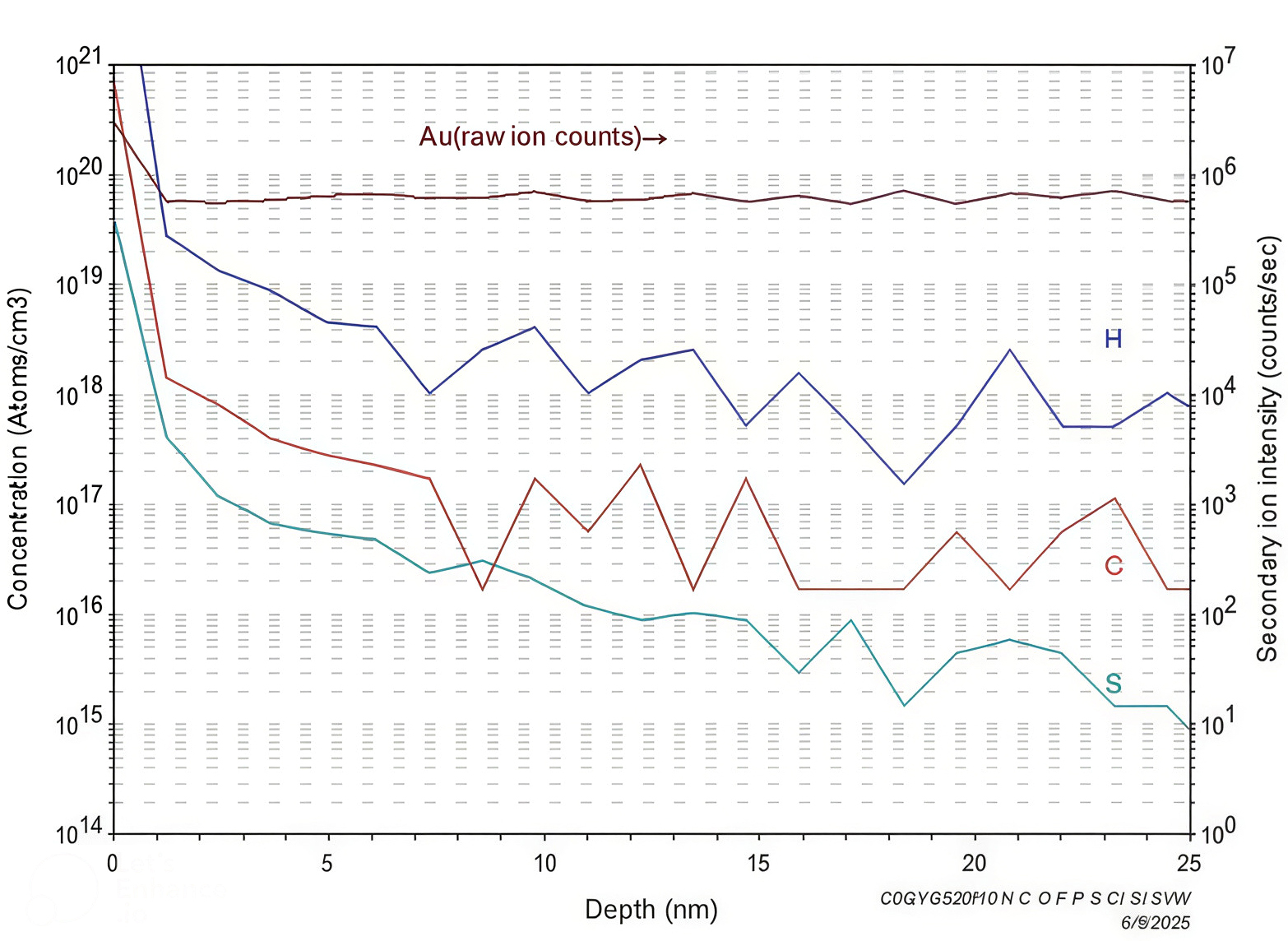
Figure 6. TOF-SIMS elemental species surface analysis.
Commentary on Figure 6: Several elemental species are present. Of particular concern are carbon (C), hydrogen (H), and sulfur (S), which were found in higher concentrations at the gold surface’s uppermost nanometers, as shown by the elevated atom density/cm3 on the graph’s left side. These elements can hinder solder wetting. The sulfur, detected in negative ion mode (spectra not shown) is attributed to benzylsulfonates (anionic surfactants commonly used in detergents). Fatty acid ions, often found in soaps, surfactants, and release agents, were also detected. These compounds can inhibit solder wetting. The presence of carbon, hydrogen, sulfur, and benzylsulfonates on the gold surface indicates possible issues with rinsing, handling, packaging, or storage. These contaminants can negatively impact soldering, and should be considered process indicators.
During soldering, flux in the paste removes contaminants and oxides from component leads and PCB pads, prevents further oxide formation, and improves wetting. It also acts as a heat bridge, transferring heat to the solder. Flux has limits, so clean PCBs remain critical.
Solder
The second member of the trinity is Solder. This member involves the correct type, the right amount, and uniform application of solder paste. The optimal volume of solder paste is crucial for long-term solder joint reliability [7].
Insufficient paste volume produces poorly formed solder joints. Starved solder joints lack sufficient fillets, which causes nonwetting and incomplete joints. Insufficient solder joints can cause latent defects.
Excessive paste volume can cause solder bridging between pads or pins, resulting in electrical shorts. Large paste volumes on small components can produce mid-chip solder beads. These are small beads that form next to chip components after reflow. Excessive paste can also cause components to float or lift during reflow, increasing standoff and potentially creating open connections on some pads.
The IPC-7525C Stencil Design Guidelines provides guidance for the design and fabrication of stencils for solder paste and surface-mount adhesive. It is intended as a guideline only. Much of the content is based on the experience of stencil designers, fabricators, and users. Printing performance depends on many different variables, and therefore, no single set of design rules can be established. Nothing in this document is mandatory unless it is specified as such in the contract documentation [8].
A general rule of thumb for SMT pads is to apply solder paste to a thickness of 0.10 mm to 0.20 mm, covering 50% to 70% of the pad. There are other methods to calculate the required solder paste volume. One such method is the Stencil Coach [9]. Printed solder paste should be inspected with a solder paste inspection system (SPI) before reflow.
Solder Paste Inspection is a process that assesses the quality of the printed solder paste deposit on the PCB prior to reflow. Inspection ensures the correct deposition of solder paste on the board without defects, as shown in Figure 7 [10]. In many cases, soldering defects are caused by improper printing of solder paste. Solder paste inspection is therefore critical.
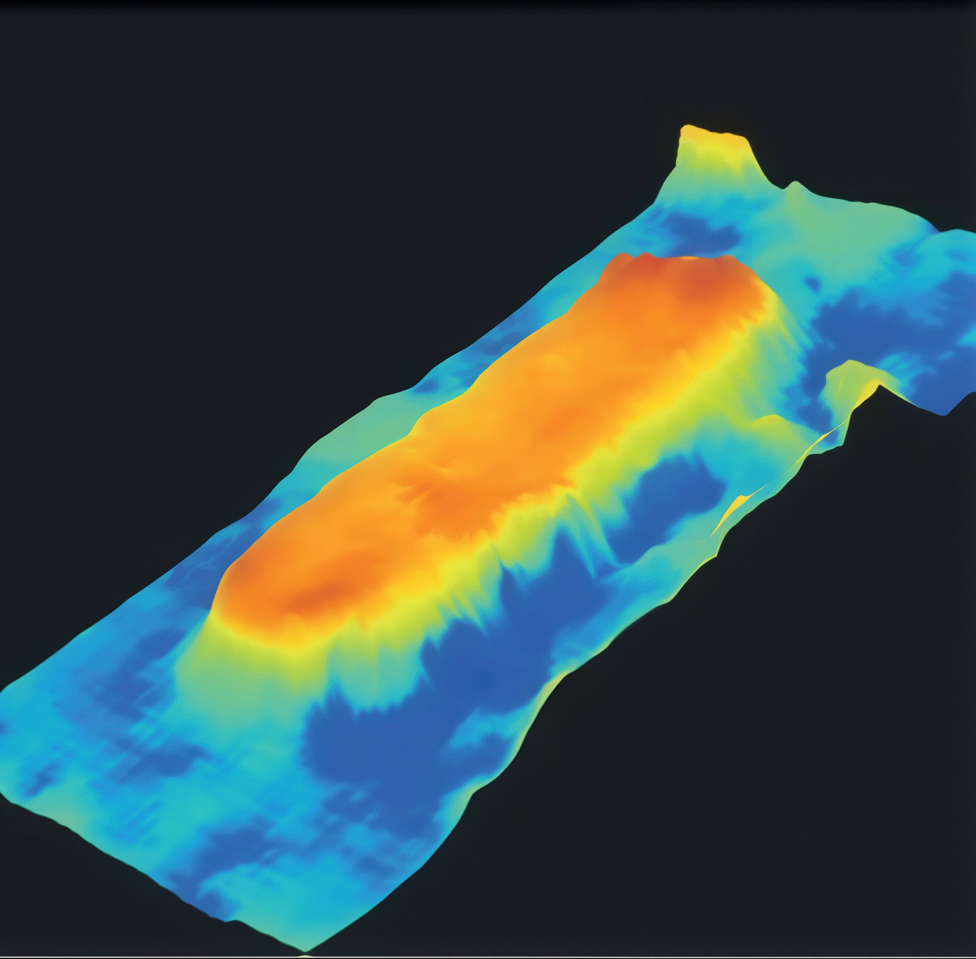
Figure 7. 3D solder paste inspection
Heat
Heat is the third member of the trinity. It includes the correct temperature, correct time, uniform heat distribution, and correct cool-down rate. The proper control of heat and cool-down is accomplished using a reflow profile. The most critical parameters are the peak temperature and the time above liquidous (TAL) as this controls liquid spreading of the solder and formation and thickness of the intermetallic compound (IMC). Figure 8 shows a typical SAC305 reflow profile [11].
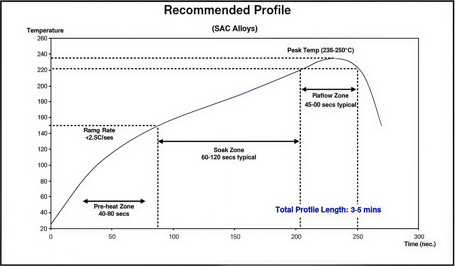
Figure 8. Typical SAC305 alloy reflow profile.
Insufficient heat causes cold connections (cold solder joints). These create weak mechanical joints and poor electrical conductivity. Low peak temperature or short time above liquidous (TAL) usually causes this. Insufficient heat also leads to latent defects.
Excessive heat can cause component failures, PCB damage, and solder joint fractures. Improper reflow profiles are usually to blame. Excessive heat can also lead to latent defects.
The cool-down rate affects the grain structure of the solder joint. A rapid (steep-slope) cool-down generally produces a small, shiny, strong solder grain structure. The rapid cool-down promotes rapid solder solidification, thereby mitigating void formation. A too-slow cool-down rate generally creates a large, duller, softer solder grain structure [12, 13].
Conclusions
Soldering converts bare PCBs into functional assemblies. Poor soldering becomes a liability issue. To be successful, maintaining strict control of the holy trinity is required: Clean, Solder, and Heat. Even extremely thin surface contaminants (1–2 nm) can disrupt soldering. Optimal solder paste volume is key for reliable solder joints. Proper heat and cool-down rates depend on instituting the correct reflow profile for the solder alloyed used. Proper soldering enables world-class quality "on target with minimal variation."
References
[1] Xu, F., et al. (2015). To Qualify a Wetting Balance Curve. Available from: https://www.electronics.org/system/files/technical_resource/E39%26S19_02%20-%20Frank%20Xu.pdf (accessed 3 January 2026).
[2] IPC-T-50 – Terms and Definitions.
[3] J-STD-003D – Solderability Tests for Printed Circuit Boards.
IPC-A-610J – Acceptability of Electronic Assemblies
[5] EAG Laboratories: SMART (Spectroscopy and Microscopy Analytical Resolution Tool) Chart. Available from: https://www.eurofins.com/materials-and-engineering-sciences/techniques/ (accessed 5 Feb 2026).
[6] Robinson, K. J. & Thissen, H. Selecting the best surface analysis method for your materials/samples. J. Vac. Sci. Technol. A 1 July 2024; 42 (4): 040801.
[7] Lentz, T., et al. (2018). How Does Printed Solder Paste Volume Affect Solder Joint Reliability? Proceedings of SMTA International, Oct. 14 - 18, 2018, Rosemont, IL, USA.
[8] IPC-7525 – Stencil Design Guidelines.
[9] Indium Corporation, Laskey, R., Dr. Stencil Coach™ Calculates Optimal Solder Paste Printing Aperture Parameters: Now Available Online. Available from: https://www.indium.com/blog/stencil-coach-calculates-optimal-solder-paste-printing-aperture-parameters-now-available-online/ (accessed 9 Jan 2026).
[10] Viscom Vision Technology: Solder paste inspection. Available from: https://www.viscom.com/en-us/products/solder-paste-inspection-3d-spi/paste-inspection-is6052-spi/ (accessed 9 Jan 2026).
[11] Kester: Recommended Reflow Profile. Available from: https://www.kester.com/ (accessed 24 Jan 2026).
[12] Indium Corporation: Stages of a Reflow Profile: Part IV. Available from: https://www.indium.com/blog/stages-of-a-reflow-profile-part-iv/ (accessed 22 Jan 2026).
[13] O’Brien, G., ST and S Group. Personal communication, 3 Nov 2025.