By Kazuki Yoshikawa, Toshiaki Shibata, Masayuki Kiso and Shigeo Hashimoto
C.Uyemura & Co., Ltd. Central Research Laboratory, Osaka Japan
By Don Gudeczaukas
Uyemura International Corporation
Southington CT
Abstract
Thermal diffusion of Ni-P/Pd/Au deposits for wire bonding reliability was studied. Palladium was used in an attempt to decrease nickel diffusion into the surface gold deposit. Transmission Electron Microscopy, FE-SEM, Auger analysis and wire bond analysis were used to measure the reliability of the finishes discussed. The test results show the controlled Ni-P/Pd/Au deposit exhibits excellent reliability for wire bonding.
Introduction
Palladium deposits are excellent barriers that prevent nickel from diffusing into gold. In this paper, electroless palladium deposits were analyzed by TEM and thermal diffusion of each element of Ni, Pd, and Au from the electroless Ni-P/Pd/Au deposit was examined. From this study, it was determined that the palladium deposit could prevent diffusion of underlying nickel to gold even when the palladium deposit is comparatively thin (about 0.06µm) and provides excellent wire bonding reliability.
Test Results
Coupons consisted of Al-Cu (0.5%) sputtered wafers (1mm thick) for the thermal diffusion test. For wire bonding reliability tests, 1mm thickness of Al-Si(1%)-Cu(0.5%) sputtered wafers which have 150µm square pads by Si-N were used. The coupons were plated using plating chemicals commercially available from C. Uyemura & Co., Ltd. Table 1(a) shows the Ni-P/Au (ENIG) plating process. Table 1(b) shows the Ni-P/Pd/Au (ENEPIG) plating process.
Table-1(a): ENIG plating process...
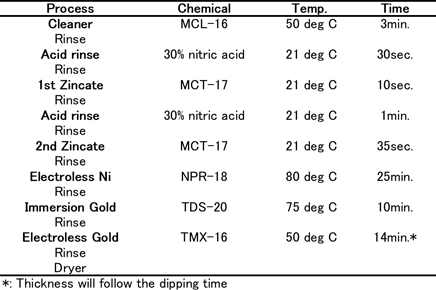
Table-1(b): ENIG plating process...
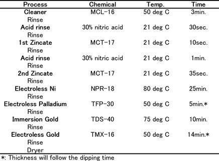
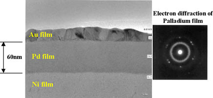
Plating thicknesses of Ni = 5µm, Pd = 0.06µm, Au = 0.02 µm were adopted. Pd and Au deposit thicknesses were adjusted as required. It was assumed that the ENEPIG deposit characteristics would greatly depend on the feature (uniformity and existence of defects) of palladium and gold deposits. Therefore, the feature of the Pd and Au deposits were confirmed by TEM, the results of which are shown in Fig. 1. By this TEM analysis result, it was confirmed that the palladium deposit is an amorphous, smooth, and uniform layer. Since the Au deposit has the crystalline plane observed, it was confirmed that the Au deposit is crystallized.
Figure 1: TEM analysis results of ENEPIG film...
To confirm the deposit surface morphology, the gold surfaces with and without heat treatment at 175°C for 16 hours were observed by FE-SEM, the results of which are shown in Fig. 2.
Figure 2: FE-SEM image of gold surface...
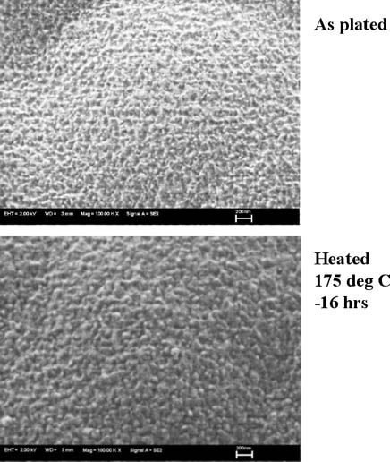
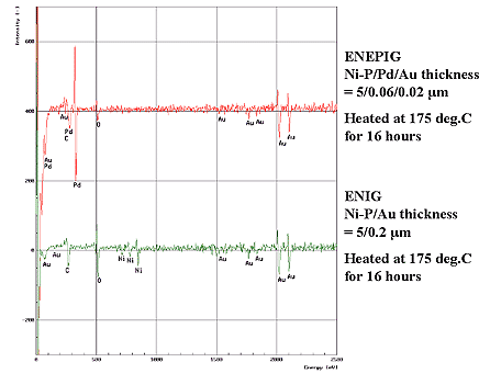
The gold surface morphologies shown in Fig. 2 coincide with the cross-sectional image of the gold layer by TEM analysis and indicate few defects, and it is confirmed that gold grain size is increased by heat treatment. Next, in order to confirm diffusion of each element by heat treatment, Ni=5µm / Pd=0.06µm / Au=0.02µm deposits and Ni=5µm /Au= 0.2µm deposits were heated at 175°C for 16 hours and the gold top surface was compared and analyzed by AES. As a result, it was clarified that by inserting the palladium deposit as thin as 0.06µm between the EN deposit and Au layers, diffusion of nickel to the gold deposit can be prevented. Results are shown in Fig. 3.
Figure 3: Comparison of ENEPIG and ENIG in AES analysis after heated at 175°C for 16 hours...
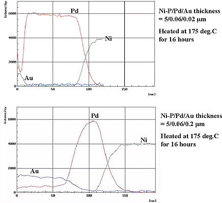
Furthermore, two types of deposits with varying gold thicknesses such as Ni=5µm / Pd=0.06µm / Au=0.02µm and Ni=5µm / Pd=0.06µm / Au=0.2µm were checked for diffusion of palladium to gold using AES-depth analysis after heating at 175°C for 16 hours. Results are shown in Fig. 4. As shown, palladium diffuses comparatively uniformly in the depth direction of the gold deposit and the Pd content in the gold film varies dependently on the gold film thickness. It is considered that the change in gold surface morphology by heat treatment shown in Fig. 2 is attributed to alloying of gold and palladium shown in Fig. 4.
Figure 4: Results of Au and Pd diffussion by AES analysis...
Evaluations of electroless ENEPIG deposits and wire bonding characteristics were performed for wafer application.
Ni-P/Pd/Au and Ni-P/Au layers were deposited on 150µm square pads and 1st bonds were performed on them. The bonding bumps were sheared by a shear tool and shear strength and failure mode were observed.
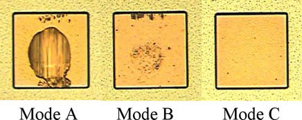
1st wire bonding conditions are shown in Table 2, shear conditions are shown in Table 3, and the failure mode is shown in Fig. 5. (Mode A: Tear between bonding ball. Mode B: Tear between bonding ball and the gold surface. Mode C: No adhesion between bonding ball and the gold surface.)
Table 2: 1st bonding test condition...
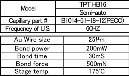
Table 3: Bond shear test condition...

Figure 5: The failure mode of 1st bond shear test results...
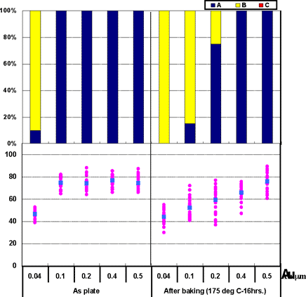
Coupons were prepared with Au thicknesses of 0.04µm, 0.1µm, 0.2µm, 0.4µm, and 0.5µm for ENIG deposits. 1st bonds were evaluated by the use of coupons before and after heating at 175°C for 16 hours.
The 1st bonding evaluation results shown in Fig. 6. As shown in Fig. 6, with the ENIG film, excellent wire bonding reliability was obtained when the Au thickness is greater than 0.4µm; however, wire bonding reliability decreases with the Au thickness less than 0.2µm. These characteristics coincide with estimated results from the Fig.3 data from Au surface analysis (Ni detection).
Figure 6: 1st bond shear test results on ENIG film...
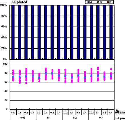
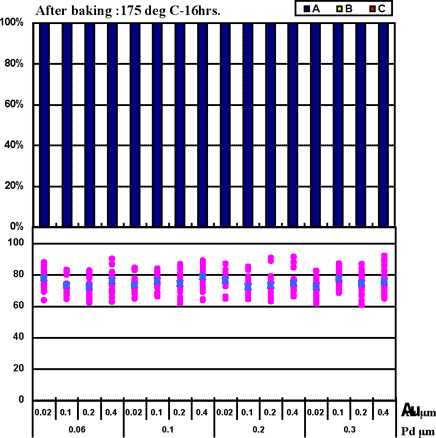
Coupons were prepared by combining Pd thicknesses of 0.06µm, 0.1µm, 0.2µm, and 0.3µm with gold deposit thicknesses of 0.02µm, 0.1µm, 0.2µm, and 0.4µm for the ENEPIG film. 1st bonds were evaluated by the use of coupons before and after heating at 175°C for 16 hours. The 1st bond evaluation results are shown in Fig. 7.
Fig. 7 shows that even if 0.02µm of Au thickness and 0.06µm of Pd thickness are implemented, excellent wire bonding reliability was obtained with the ENEPIG deposit. The characteristics coincide with estimated results from the Fig.3 data from Au surface analysis (no Ni detection).
Figure 7: 1st bond shear test results on ENEPIG film...
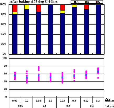
It was confirmed the wire bonding characteristicsdepended on Au thickness and heat treatment with Ni-P/Au film. However, we did not confirm similar results with the Ni-P/Pd/Au film. Therefore, in decreasing the bond power to 130mW, 1st bonding characteristics were observed with each thickness of Pd and Au film shown in Fig.8.
As shown in Fig.8, thicker Au produced better wire bonding characteristics without dependence on the Pd film thickness under low bond power.
Figure 7: 1st bond shear test results on ENEPIG film (Bond power 130mW)...
Summary
In this report, heat diffusion of each element in the ENEPIG film was investigated and it was found that diffusion of Ni to gold can be prevented by insertion of an approximately 0.06mm thick electroless palladium layer between Au and EN deposits.
Based on the results, even if the gold thickness of Ni-P/Pd/Au deposit was 0.02µm, excellent wire bonding characteristics were obtained. Thicker Au produced better wire bonding characteristics without dependence on the Pd film thickness under low bond power. Excellent wire bonding characteristics were obtained by depositing thicker Au with Ni-P/Au deposits which could better withstand thermal aging.